Introduction to DSown Evaluation Boards
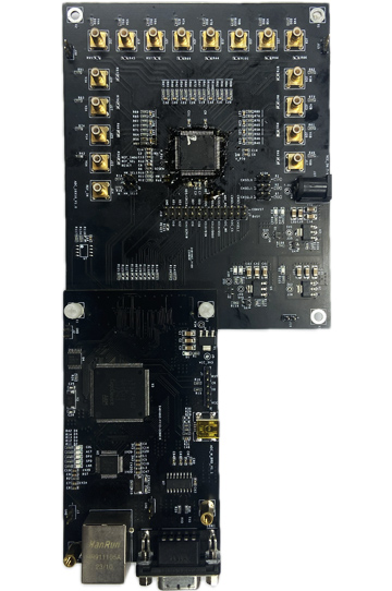
ADCP9653E-125 Evaluation Board and Introduction
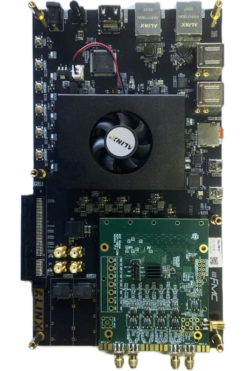
- The ADCP9653E-125 evaluation board from DSown adopts a configuration of an FPGA mainboard combined with an FMC daughterboard (high-speed ADC board).
- The FPGA mainboard is a development board based on the XILINX ZYNQ7000 platform (model: AX7350B).
- This ZYNQ7000 FPGA development platform uses the XILINX ZYNQ7000 SoC chip XC7Z035, which integrates dual-core ARM Cortex-A9 processors and FPGA programmable logic on a single chip through ARM+FPGA SoC technology.
- Both the PS (Processing System) and PL (Programmable Logic) sides of the ZYNQ are equipped with two 512MB high-speed DDR3 SDRAM chips each. Additionally, the PS side includes an 8GB eMMC storage chip and a 256Mb QSPI FLASH chip.
- The FPGA development platform provides a rich set of interfaces: 1 PCIe x4 slot, 2 optical fiber interfaces, 2 Gigabit Ethernet interfaces, 4 USB 2.0 HOST ports, 1 HDMI output, 1 UART serial port, 1 SD card interface, and an FMC expansion interface.
- The ADCP9653E-125 data acquisition daughterboard connects to the FPGA mainboard via a standard FMC interface. The acquisition board supports 4-channel data acquisition and includes a reserved external clock input interface, allowing users to select either an external or onboard clock source.
Core Specifications of the ADCP9653E-125 Chip:
-Supply Voltage: 1.8VLow Power
-Consumption: 164 mW per channel
-Signal-to-Noise Ratio (SNR):
76.5 dB S (at 70 MHz, 2.0 V p-p input range)
77.5 dB S (at 70 MHz, 2.6 V p-p input range)
-Spurious-Free Dynamic Range (SFDR): 90 dBc (up to Nyquist, 2.0 V p-p input range)
-Differential Nonlinearity (DNL): ±0.7 LSB
-Consumption: 164 mW per channel
-Signal-to-Noise Ratio (SNR):
76.5 dB S (at 70 MHz, 2.0 V p-p input range)
77.5 dB S (at 70 MHz, 2.6 V p-p input range)
-Spurious-Free Dynamic Range (SFDR): 90 dBc (up to Nyquist, 2.0 V p-p input range)
-Differential Nonlinearity (DNL): ±0.7 LSB
-Integral Nonlinearity (INL): ±3.5 LSB (2.0 V p-p input range)
-Serial LVDS interface, low-power, reduced-range option
-Full-power analog bandwidth: 650 MHz
-Input voltage range: 2 V p-p (supports up to 2.6 V p-p)
-Serial port control
-Serial LVDS interface, low-power, reduced-range option
-Full-power analog bandwidth: 650 MHz
-Input voltage range: 2 V p-p (supports up to 2.6 V p-p)
-Serial port control
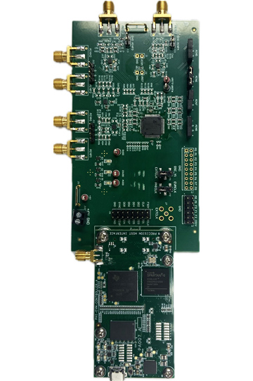
DAD9783 Evaluation Board and Introduction
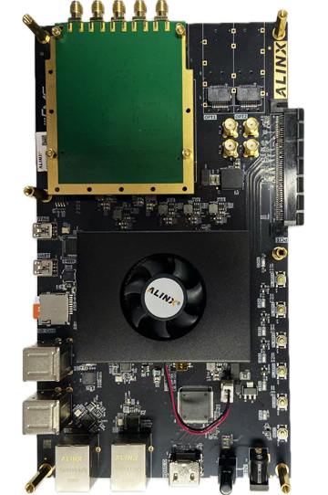
- The DAD9783 development board from Dsown adopts a configuration of an FPGA mainboard combined with an FMC daughterboard (high-speed DAC board).
- The FPGA mainboard is a development board based on the XILINX ZYNQ7000 platform (model: AX7350B).
- This ZYNQ7000 FPGA development platform uses the XILINX ZYNQ7000 SoC chip XC7Z035, which integrates dual-core ARM Cortex-A9 processors and FPGA programmable logic on a single chip through ARM+FPGA SoC technology.
- Both the PS (Processing System) and PL (Programmable Logic) sides of the ZYNQ are equipped with two 512MB high-speed DDR3 SDRAM chips each. Additionally, the PS side includes an 8GB eMMC storage chip and a 256Mb QSPI FLASH chip.
- The FPGA development platform provides a rich set of interfaces: 1 PCIe x4 slot, 2 optical fiber interfaces, 2 Gigabit Ethernet interfaces, 4 USB 2.0 HOST ports, 1 HDMI output, 1 UART serial port, 1 SD card interface, and an FMC expansion interface.
- The DAD9783 analog output daughterboard connects to the FPGA mainboard via a standard FMC interface. The board outputs two analog signals, IOUT and QOUT, and includes a reserved external clock input interface, allowing users to select either an external or onboard clock source.
Core Specifications of the DAD9783 Chip:
-High dynamic range, dual DAC architecture
-Low noise and intermodulation distortion
-Single-carrier W-CDMA ACLR: 80 dBc (at 61.44 MHz)
-Innovative switching output stage allowing output frequencies beyond the Nyquist rate
-LVDS input with dual-port operation or optional interleaved single-port mode
-Programmable differential analog current output:
8.6 mA – 31.7 mA full-scale range
-Auxiliary 10-bit current DAC with sourcing and sinking capability for external offset zero-point calibration
-Integrated 1.2V precision voltage reference
-Operating supply voltage: 1.8V to 3.3V
-Power consumption: 320 mW
-Package type: QFN72
-Integrated 1.2V precision voltage reference
-Operating supply voltage: 1.8V to 3.3V
-Power consumption: 320 mW
-Package type: QFN72
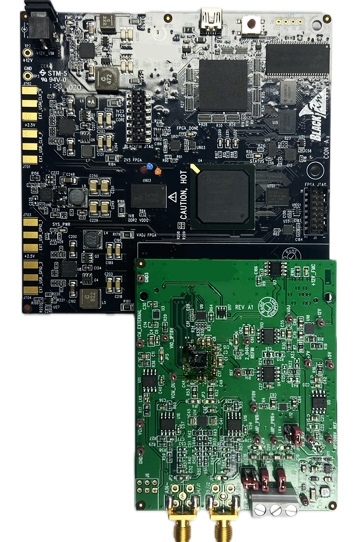
DAD9747 Evaluation Board and Introduction
- The Dsown DAD9747 Evaluation Board adopts a modular design consisting of an FPGA main board and an FMC daughter card (high-speed DAC board).
- The FPGA main board is based on the XILINX ZYNQ-7Z020 development platform, which utilizes the XILINX ZYNQ SoC XC7Z020 solution. This SoC integrates a dual-core ARM Cortex-A9 processor with FPGA programmable logic in a single chip using ARM+FPGA SoC architecture.
- This FPGA platform offers flexible interfaces and a wide range of peripherals, featuring an on-board standard FMC-LPC connector that supports various FMC daughter modules.
- The DAD9747 FMC daughter card connects to the FPGA main board via the FMC interface. It provides dedicated DCO and CLK_IN interfaces for external clock sources, while the OUT1 and OUT2 output channels use SMA connectors for convenient signal testing.
- Comprehensive reference schematics, FPGA test code, and brief test documentation are provided to help users with setup and debugging.
Core Specifications of the DAD9747 Chip:
-High dynamic range, dual DAC architecture
-Low noise and intermodulation distortion
-Single-carrier W-CDMA ACLR: 80 dBc (at 61.55 MHz)
-Innovative switching output stage allowing output frequencies beyond the Nyquist rate
-Dual-port LVCMOS input with optional cross-access single-port operation
-Programmable differential analog current output:
8.6 mA – 31.7 mA
-Auxiliary 10-bit current DAC with sourcing/sinking capability, suitable for external offset compensation circuits
-Built-in 1.2 V precision reference voltage
-Operating voltage: 1.8 V – 3.3 V
-Power consumption: 320 Mw
-Package: QFN72
-Built-in 1.2 V precision reference voltage
-Operating voltage: 1.8 V – 3.3 V
-Power consumption: 320 Mw
-Package: QFN72
DAD7606 Evaluation Board and Introduction
- The Dsown DAD7606 Evaluation Board adopts a modular design with an MCU main board and an ADC daughter board.
- The main board features the GD32F450 microcontroller and includes on-board connectors for serial port, Ethernet, and SWD interfaces, providing flexibility for user debugging.
- The DAD7606 daughter board is powered through a 7.5V DC input jack and can be controlled via an on-board switch.
- Test points on the DAD7606 daughter board include: SPI interface, BUSY pin, CONVST pin, VCC, and GND.
- The interface method (parallel or serial) can be selected using 0-ohm resistors for easy configuration. Additionally, over-sampling can be configured via 0-ohm resistors.
- All input channel pins are available for easy connection, and the board allows users to configure VxGND via jumpers to choose between single-ended input or differential input.
- Comprehensive reference schematics, engineering test code, and evaluation board testing instructions are included to support users in debugging and integration.
Core Specifications of the DAD7606 Chip:
-Single power supply operation: 2.5V to 5.5V
-8 synchronous sampling inputs
-True bipolar analog input range: ±10V, ±5V
-5V single analog supply, with V DRIVE power
-supply voltage: 2.3V to 5.5V
-16-bit, 200kSPS ADC for all channels
-Oversampling functionality provided by digital filters
-Flexible parallel and serial interfaces
-8 synchronous sampling inputs
-True bipolar analog input range: ±10V, ±5V
-5V single analog supply, with V DRIVE power
-supply voltage: 2.3V to 5.5V
-16-bit, 200kSPS ADC for all channels
-Oversampling functionality provided by digital filters
-Flexible parallel and serial interfaces
-Signal-to-Noise Ratio (SNR): 89 dB
-Total Harmonic Distortion (THD): –106 dB
-INL: ±0.5 LSB DNL: ±0.5 LSB
-Low Power Consumption: 90 mW
-Package: 64-LQFP
-Total Harmonic Distortion (THD): –106 dB
-INL: ±0.5 LSB DNL: ±0.5 LSB
-Low Power Consumption: 90 mW
-Package: 64-LQFP
DAD7616 Evaluation Board and Introduction
- The Dsown DAD7616 Evaluation Board features a modular design with an MCU main board and an ADC daughter board.
- The main board is powered by the GD32F450 microcontroller and includes onboard serial, Ethernet, and SWD interfaces, providing flexibility for user debugging.
- The ADC daughter board is powered via a 7.5V DC input jack.
- Test points on the DAD7616 daughter board include: SPI interface, BUSY pin, CONVST pin, STBY pin, VCC, and GND.
- The ADC operating mode (hardware or software) can be selected via 0-ohm resistors, and the interface type (parallel or serial) can also be configured using 0-ohm resistors.
- Comprehensive reference schematics, engineering test code, and evaluation board testing instructions are provided to facilitate debugging and integration.
Core Specifications of the DAD7616 Chip:
-16 channels, dual simultaneous sampling inputs
-Independently selectable input ranges per channel:
True bipolar ±10V, ±5V, ±2.5V
-5V single analog supply, with V DRIVE voltage:
2.3V to 5.5V
-Dual-channel 16-bit Successive Approximation
Register (SAR) ADCs
-Throughput rate: 2 × 1 MSPS
-Independently selectable input ranges per channel:
True bipolar ±10V, ±5V, ±2.5V
-5V single analog supply, with V DRIVE voltage:
2.3V to 5.5V
-Dual-channel 16-bit Successive Approximation
Register (SAR) ADCs
-Throughput rate: 2 × 1 MSPS
-Flexible sequencer supporting burst mode operation
-Flexible parallel and serial interfaces
-Signal-to-Noise Ratio (SNR): 90.5 dB
-Total Harmonic Distortion (THD): –101 dB
-INL: ±1 LSB DNL: ±0.99 LSB
-Low Power Consumption: 150 mW
-Package Type: 80-LQFP
-Flexible parallel and serial interfaces
-Signal-to-Noise Ratio (SNR): 90.5 dB
-Total Harmonic Distortion (THD): –101 dB
-INL: ±1 LSB DNL: ±0.99 LSB
-Low Power Consumption: 150 mW
-Package Type: 80-LQFP
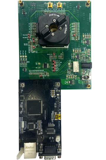
DADS1278-C/1274-C Evaluation Board and Introduction
- The Dsown DADS1278-C/1274-C Evaluation Board adopts a main board + ADC data acquisition daughter board architecture.
- The main board utilizes an ARM + XILINX FPGA design and connects to a PC via a USB interface for digital input and output operations.
- The DADS1278-C data acquisition daughter board provides data acquisition connectors and jumper settings, allowing flexible configuration of clock sources, single-ended, or differential input modes.
- Comprehensive reference schematics, evaluation software, and testing documentation are provided to assist users with evaluation and system integration.
Core Specifications of the DADS1278-C/1274-C Chip:
-8/4 channel simultaneous measurement
-Maximum sampling rate: 144 kSPS
-AC performance: 70 kHz bandwidth /
110 dB SNR / –109 dB THD
-DC accuracy: 0.8 μV/°C offset drift / 1.3 ppm/ °C gain drift
-Selectable operating modes:
High Speed: 144 kSPS, 106 dB SNR
High Resolution: 52 kSPS, 110 dB SNR
Low Power: 52 kSPS, 38 mW per channel
Low Speed: 10 kSPS, 8.4 mW per channel
-Built-in linear digital filtering
-SPI or synchronous frame serial interface
-Low aperture error
-Supports modulator output mode
-Package type: TQFP-64
-SPI or synchronous frame serial interface
-Low aperture error
-Supports modulator output mode
-Package type: TQFP-64
DAD7960 Evaluation Board and Introduction
- The Dsown DAD7960 Evaluation Board features a FPGA + DSP main board combined with an ADC data acquisition daughter board.
- The main board integrates a XILINX FPGA and an ADSP-BF527 processor, and connects to a PC via a USB interface, allowing users to configure the daughter board and acquire data directly from the PC.
- The DAD7960 data acquisition daughter board connects to the main board via an FMC interface.
- Comprehensive reference schematics, PC software, and evaluation board manuals are provided to facilitate user evaluation and testing.
Core Specifications of the DAD7960 Chip:
-18-bit, 5 MSPS, SAR ADC
-Dynamic Range (DR): 100 dB
-Signal-to-Noise Ratio (SNR): 99 dB
-Spurious-Free Dynamic Range (SFDR): 115 dB
-Total Harmonic Distortion (THD): –117 dB
-Integral Nonlinearity (INL): ±2 LSB
-Differential Nonlinearity (DNL): ±0.99 LSB
-Low Power Consumption: 64.5 mW
-Supply Voltage: 1.8 V / 5.0 V
-Dynamic Range (DR): 100 dB
-Signal-to-Noise Ratio (SNR): 99 dB
-Spurious-Free Dynamic Range (SFDR): 115 dB
-Total Harmonic Distortion (THD): –117 dB
-Integral Nonlinearity (INL): ±2 LSB
-Differential Nonlinearity (DNL): ±0.99 LSB
-Low Power Consumption: 64.5 mW
-Supply Voltage: 1.8 V / 5.0 V
-Differential analog input range:
Supports ±VREF (any input within 0V to +VREF)
-Maximum VREF: 5 V, typical 4.096 V – 5 V
-Digital logic interface: 1.8 V
-Serial LVDS interface
-Operating temperature range:
–40°C to +85°C
-Package type: QFN32
Supports ±VREF (any input within 0V to +VREF)
-Maximum VREF: 5 V, typical 4.096 V – 5 V
-Digital logic interface: 1.8 V
-Serial LVDS interface
-Operating temperature range:
–40°C to +85°C
-Package type: QFN32
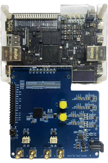
DADS1220/1120 Evaluation Board and Introduction
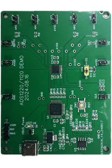
- The Dsown DADS1220/1120 Evaluation Board adopts a STM8 microcontroller main board + onboard ADC architecture.
- The evaluation board provides an SWD interface for easy code debugging and verification.
- An integrated USB-to-serial chip allows PC communication via a USB-C interface, eliminating the need for a separate serial cable and simplifying user testing.
- The DADS1220/1120 chip provides dedicated interfaces including AVDD, REF, AVSS, CLK, and AIN0~AIN3 input channels, facilitating flexible signal testing and debugging.
- The power supply mode of the DADS1220/1120 can be configured via jumpers to support single-supply or dual-supply operation.
- Comprehensive reference schematics, engineering test code, and evaluation board manuals are provided to support user debugging and system integration.
Core Specifications of the DADS1220/1120 Chip:
-Low current consumption: as low as 120 μA in
duty-cycle mode
-Wide supply voltage range: 2.3 V to 5.5 V
-Programmable gain: 1 V/V to 128 V/V
-Programmable data rate: up to 2 kSPS
-Noise-free resolution: up to 20-bit / 16-bit
(DADS1220/1120)
-Single-cycle settling digital filter providing 50 Hz
and 60 Hz harmonic rejection at 20 SPS
-Input configuration: two differential inputs or four
single-ended inputs
-Dual matched programmable current sources: 10 μA to 1.5 mA (DADS1220) / 50 μA to 1.5 mA (DADS1120)
-Integrated 2.048 V voltage reference: 5 ppm/°C drift (typical)
-Integrated 2% precision oscillator
-Integrated temperature sensor: 0.5°C accuracy (typical)
-SPI-compatible interface
-Integrated 2.048 V voltage reference: 5 ppm/°C drift (typical)
-Integrated 2% precision oscillator
-Integrated temperature sensor: 0.5°C accuracy (typical)
-SPI-compatible interface