High-Performance Bioelectric Signal Acquisition Tool — Input Impedance Analysis and Measurement Methods of the DADS1299

In fields such as EEG (electroencephalography), BCI (brain–computer interface), and neuroscience research, signal amplitudes are typically on the order of tens of microvolts—extremely weak by nature. Under these conditions, the performance of the front-end acquisition IC is critical, and input impedance is one of the key parameters that directly determines signal integrity.
The DADS1299, developed by DSown Technology, is a high-precision 24-bit analog-to-digital converter specifically designed for bioelectric signal acquisition. It features high input impedance, low noise, and comprehensive impedance detection capabilities, providing an ideal hardware foundation for applications such as EEG, ECG, and ECoG.
This article presents an in-depth analysis of the input impedance characteristics of the DADS1299 and explains how to perform impedance measurements using its integrated features.
What Is Input Impedance?
Input impedance refers to the impedance “seen” by the signal source at the front-end interface. In weak-signal acquisition systems, insufficient input impedance can lead to several issues:
- Signal attenuation and voltage division distortion.
- Unstable electrode–skin contact, resulting in amplified noise.
- Degraded common-mode rejection performance of the system.
Input Impedance Characteristics of the DADS1299
The DADS1299 integrates a low-noise front-end programmable gain amplifier (PGA). Under normal operating conditions, it achieves a typical input impedance on the order of 1 GΩ—significantly higher than typical electrode impedances (ranging from a few kilo-ohms to tens of kilo-ohms).
Key features include:
Key features include:
- High input impedance: Ensures that ultra-weak signals (e.g., EEG) are not significantly attenuated due to electrode impedance.
- Programmable gain (PGA): Supports gain settings from 1 to 24, enabling flexible adaptation to different experimental conditions.
- Low noise performance: Within a 0.01–70 Hz bandwidth and at a gain of 24, the typical input-referred noise is only 1.35 μVpp.
- Bias drive circuitry: Effectively suppresses common-mode interference, improving overall signal-to-noise ratio (SNR).
Why Is High Input Impedance Important?
Consider a simple example: if the electrode impedance is 50 kΩ and the chip’s input impedance is 1 GΩ, the voltage division ratio is approximately:
50k / (50k + 1G) ≈ 0.005%
This level of attenuation is practically negligible. However, if a low-input-impedance amplifier is used instead, the signal would be significantly attenuated, potentially impacting subsequent feature extraction and analysis.
The high input impedance of the DADS1299 provides a robust foundation for accurate acquisition of weak bioelectric signals.
Electrode Impedance and System Design Considerations
It is important to note that while high input impedance ensures minimal signal attenuation, electrode impedance must still be maintained within a reasonable range.
Therefore, in practical applications, it is recommended to:
- Excessively high electrode impedance: Increases susceptibility to 50/60 Hz power-line interference.
- Imbalanced electrode impedance: May degrade the system’s common-mode rejection ratio (CMRR).
Therefore, in practical applications, it is recommended to:
- Use high-quality electrodes and keep impedance below 50 kΩ.
- Leverage the DADS1299's bias drive circuitry to enhance interference rejection.
- Implement proper shielding and grounding in the system design.
Impedance Measurement Method of the DADS1299
The DADS1299 integrates built-in impedance measurement functionality. It can generate a small AC excitation current and perform impedance detection directly on its input channels.
The overall process consists of three stages:
- Hardware configuration.
- Software configuration.
- Data analysis.
1.Hardware configuration

The internal current source—connected to either the P or N input (assuming here it is connected to the N input)—generates a small excitation current. This current flows through R0, R1, and R2, and then reaches the VCM node.
Due to the virtual open (high input impedance) characteristic of the operational amplifier, virtually no current flows through R4 into the N input. As a result, the differential voltage between P and N is determined by the voltage drop generated by the current flowing through R0 and R1.
This differential voltage is precisely what is measured by one channel of the ADC. Therefore, the measured voltage effectively corresponds to the combined impedance of R0 + R1.
2.Software Configuration

Impedance measurement is primarily configured via the LOFF registers. Setting the x-th bit in LOFF_SENSN enables the excitation current to be sourced from the corresponding x-th N channel. Similarly, setting the x-th bit in LOFF_SENSP enables current output from the corresponding x-th P channel.
The selected P or N channel should be configured as Normal Input to receive the AC signal generated across the impedance under test.
3.Data Analysis and Impedance Calculation
The impedance value is obtained through FFT-based analysis. As illustrated in the example, the signal consists of a DC component, a 31.2 Hz component, and a 50 Hz component. Its non-normalized FFT spectrum is shown accordingly, where:
- The horizontal axis represents frequency (Hz).
- The vertical axis represents signal magnitude in the frequency domain.
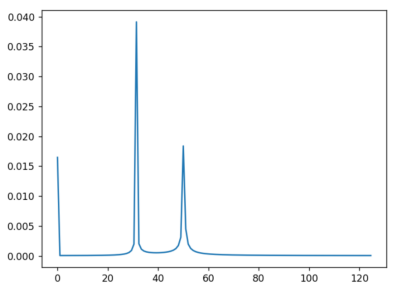
For a non-normalized FFT spectrum:
- The magnitude at 0 Hzcorresponds to the DC component. Its amplitude (i.e., DC voltage) can be calculated as:
FFT(0) / N, where N is the number of FFT points - For AC components at other frequencies, the amplitude can be calculated as:
FFT(n) / (N / 2), where nis the index of the target frequency
Once the DC or peak amplitude of the voltage signal is obtained, the impedance can be calculated using the known excitation current and Ohm’s Law.
Note that when the excitation signal is AC, the current value represents the RMS (root mean square) current. The relationship between peak and RMS current is:
Peak = * × RMS
4.Practical Considerations
The internal PGA of the DADS1299 has different input voltage ranges depending on the selected gain setting. During impedance measurement, relatively large excitation currents and high impedance values may produce input voltages that exceed the allowable input range of the ADC.
Therefore:
- The PGA gain should be adjusted בהתאם to the actual circuit conditions.
- After changing the gain, the voltage conversion formula must also be updated accordingly.
Application Value
With its high input impedance and integrated impedance measurement capabilities, the DADS1299 offers significant advantages in EEG, BCI, and neuroscience applications:
- Ensures signal integrity:Ultra-high input impedance minimizes signal attenuation.
- Improves experimental efficiency:Built-in impedance detection eliminates the need for external circuitry.
- Enhances noise immunity:Bias drive circuitry supports stable, long-term signal acquisition.
- Stable supply:DSown Technology provides technical support and long-term availability.
In EEG, BCI, and medical electronics applications, the DADS1299 serves as a stable and reliable alternative solution. For bioelectric acquisition system design, selecting the DADS1299 enables higher signal quality and improved system reliability in both research and product development.
More Information and Purchasing Channels
DSown Technology is a high-tech company specializing in the design and development of high-performance analog and mixed-signal ICs. Backed by an experienced R&D team, the company is committed to delivering leading-edge solutions tailored to various application scenarios. Its product portfolio includes four major categories:
- High-precision DACs and ADCs.
- Isolators and amplifiers.
- Industrial sensor ICs.
- Voltage reference devices.
For more information, please visit: https://dsown.com/ or contact: